The Life and Work of Konrad Zuse (by Horst Zuse)

Part 3: Konrad Zuse's First Computer -- The Z1
In 1936, my father finished the logical plan for his first computer, the V1 (he later changed the name to Z1 in order to avoid any connection with the V1 rocket). He had studied the available mechanical calculating machines of that time, all of which were based on the decimal number system. However, he never planned to build a modified or extended decimal machine, because he wanted to build a new type of computer for universal scientific applications.

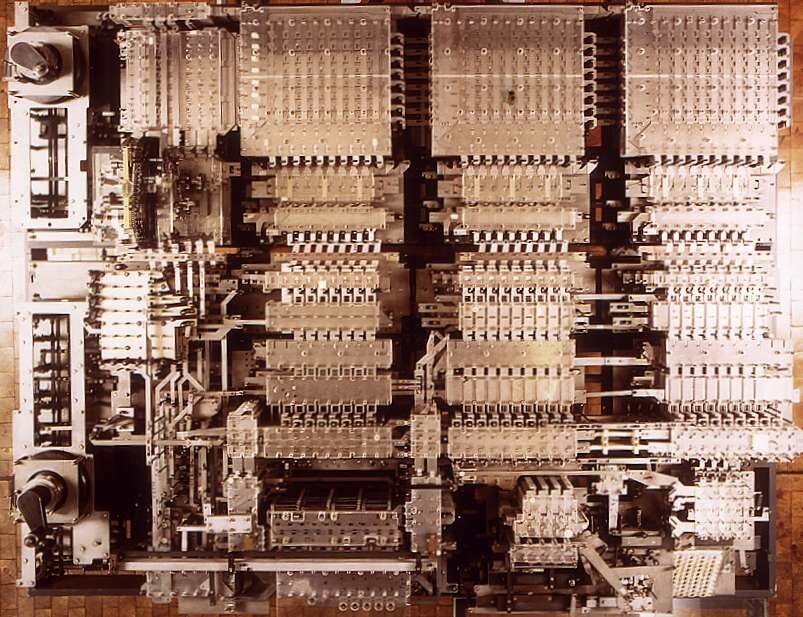
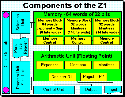
From 1936 to 1938, my father constructed the Z1, which worked on the principles discussed in Part 2. In many ways the Z1 was a remarkable machine. In addition to a 64-word memory (where each word contained 22 bits), this machine had all of the components we previously discussed in Part 2. Thus, the Z1 was the first freely programmable, binary based machine in the world!

The original Z1

The Z1 was built out of thin metal strips

Fig.7. The Z1 computer in the living room
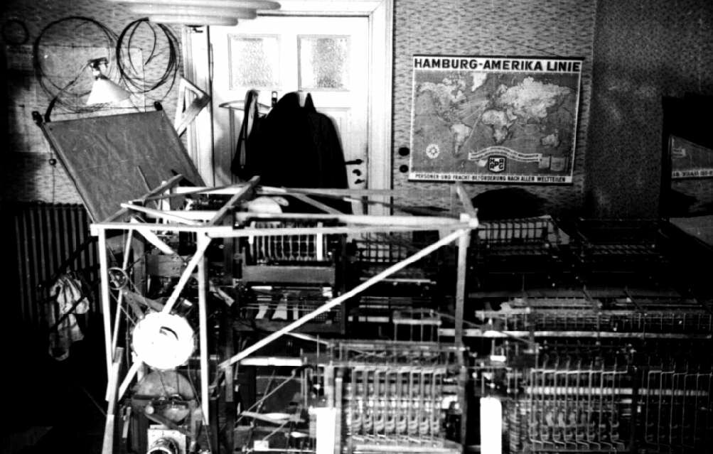
of Konrad Zuse's parents in 1936.
Fig.8. The building blocks of the Z1
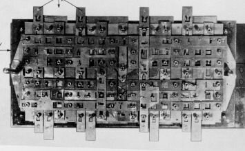
were thin metal sheets.
The Z1 did not use relays, but instead consisted completely of thin metal sheets, which he and his friends produced using a jigsaw. The only one electrical unit was an electrical engine, which was used to provide a clock frequency of one Hertz.

The Z1 was programmed via a punch tape and a punch tape reader. There was a clear separation between the punch tape reader, the control unit (which supervised the whole machine and the execution of the instructions), the arithmetic unit (with registers R1 and R2), the memory, and the input/output devices.

In 1986, Konrad Zuse decided to rebuild the Z1 (Fig. 13), because the architecture of the Z1 was almost identical to that of his Z3 computer (discussed below), which was unfortunately destroyed in the Second World War. Thus, the saying "War is the father of everything," is not true in the case of the invention of the computer.

Birds-eye view of the rebuilt Z1

Fig.9. The rebuilt Z1 seen
from a "birds-eye" view. (Source: Deutsches Technik Museum Berlin)

Note how it resembles a
modern silicon chip.

Block diagram of the Z1

Fig.10. High-level block diagram of the Z1.

Note how this block diagram maps onto the physical Z1 shown in Fig.9 (above).

Most of the components are self-explanatory. The memory, which consisted of 64 words, each containing 22 bits, was formed from three blocks. The first block contained 64 words for the exponents and signs (8 bits for each word). The other two blocks each contained 32 words for the mantissa (14 bits for each word). The selection unit interpreted the address for the memory by the control unit. The arithmetic unit was an adder, and all of the operations were reduced to additions or subtractions (adding and subtracting are very similar operations).

The registers R1 and R2 were two words, each containing 22 bits. The two circles on the left-hand side (on the clock generator block) are cranks for executing a clock cycle manually, where the upper one is for the memory and the lower one for the control and arithmetic unit.

Previous Section    Return to Index    Next Section


Copyright & Contact Info

Return to EPE Online Home Page